


Innovation: Unveiling Microsilicon Technology's Chilpet Packaging Solution
On December 11, the Shanghai Integrated Circuit 2024 Industrial Development Forum and the 30th Integrated Circuit Design Industry Exhibition opened at the Shanghai World Expo Exhibition and Convention Center. Focusing on the theme of "Smart Shanghai, a World of Chips," the event brought together experts to discuss the future landscape of the integrated circuit industry.
Unveiling Microsilicon Technology's Chilpet Packaging Solution for Silicon Bridges
On December 11th, the Shanghai Integrated Circuit 2024 Industrial Development Forum and the 30th Integrated Circuit Design Industry Exhibition opened at the Shanghai World Expo Exhibition Hall, focusing on the theme of "Smart Shanghai, Heartbeat of the World," to discuss the future of the integrated circuit industry.
In the afternoon session of the Advanced Packaging and Testing Forum on the 12th, Hangzhou Microsilicon Technology Co., Ltd. (hereinafter referred to as Microsilicon Technology), a leading domestic advanced packaging company, presented a keynote speech, "Analysis of Embedded Fan-out Silicon Bridge Packaging Solutions for Chiplets," delivered by its CTO, Wang Xin. The speech shared Microsilicon Technology's predictions and analyses of the advanced packaging industry, the company's development status and technological advancements, and importantly, launched its new Chiplet packaging technology solution, MST Fobic. Hundreds of attendees were present to hear the presentation.

Microsilicon Technology CTO Wang Xin
Major Release of Silicon Bridge Chiplet Solution, Leading a New Technological Era
With the rapid development of AI and HPC high-computing power demands, the demand for high-performance chips as computing power carriers is also increasing rapidly. However, the path to advanced processes is becoming increasingly difficult. On the one hand, the slowdown in Moore's Law iteration has led to a sharp increase in the marginal cost of chip performance growth; on the other hand, due to limitations in lithography machines, miniaturization of front-end processes is becoming increasingly difficult.
Advanced packaging is the key to surpassing Moore's Law and improving chip performance. As silicon chips approach their physical limits, the cost of improving chip performance by shrinking transistors is increasing. Advanced packaging technology, with Chiplets at its core, has become a crucial path and breakthrough for the development of integrated circuits.
At the Advanced Packaging and Testing Forum, Wang Xin analyzed various packaging technologies and pointed out that silicon bridge Chiplets will be the mainstream trend in future advanced packaging. He then focused on introducing Microsilicon Technology's new Chilpet packaging technology solution, MST Fobic.
Specifically, Microsilicon Technology's silicon bridge Chiplet utilizes Bridge Si technology to achieve sub-micrometer-level interconnection. Compared with CoWos or Interposer methods, it offers a significant cost advantage. This technology enables tighter connections between chips, helping improve performance and reduce power consumption.
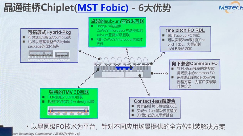
Microsilicon Technology Silicon Bridge Chiplet Packaging Technology Solution MST Fobic
TMV technology allows Microsilicon Technology's silicon bridge Chiplet to achieve 2.5D/3D interconnection, improving the connection density and performance between chips. At the same time, it avoids TSV Re-Design issues, reducing design complexity and cost.
Microsilicon Technology's silicon bridge Chiplet can flexibly implement BGA/Bump packaging methods and can also be integrated with the substrate to form a hybrid package. This optimized structure can meet the needs of different application scenarios. By using the Face up FO method, a 2um-level Fine Pitch RDL can be achieved. This high-density redistribution layer design surpasses traditional solutions such as eWLB, enabling more compact packaging designs.
In addition, Microsilicon Technology's silicon bridge Chiplet technology provides excellent die-attach and debonding methods, achieving positional accuracy on the order of ±1 micron. This is crucial for improving packaging yield and reliability.
With the continuous development of the semiconductor industry, silicon bridge Chiplets are expected to become the mainstream trend in advanced packaging. This technology, with its unique advantages such as high wiring accuracy, high package pin density, and small package size, meets the needs of high-performance computing and networking for ultra-high-density packaging.
Currently, silicon bridge Chiplet technology has been widely used in high-performance computing fields such as AI servers, AI mobile phones, and AI PCs, becoming one of the key technologies driving the development of these fields. Data shows that the market share of silicon bridge packaging solutions reached 24% in 2024 and is expected to reach 55% in 2025, indicating strong market growth potential.
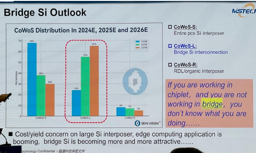
Cowos Distribution Prediction
Due to the high technical barriers, there are not many companies in China that truly master this technology, giving Microsilicon Technology a significant competitive advantage. With the continuous maturity of the technology and the expansion of the market, Microsilicon Technology is expected to achieve rapid development with its embedded fan-out silicon bridge packaging technology, creating more value for shareholders and customers.
Team Philosophy: Low-key, Pragmatic, and Efficient Progress
Achievement comes from talent; success is built on talent. Technological research and development ultimately rely on talent.
Core members of the Microsilicon Technology team have extensive experience in advanced packaging. It is reported that Microsilicon Technology is one of the earliest teams in China to deploy and research Chiplets. Through years of experience abroad, it was one of the first in China to achieve high-density wafer-level fan-out technology and independently developed the FOSiP technology route, which can meet the fan-out packaging needs for different linewidths. It has achieved fan-out packaging from ordinary linewidths to fine linewidths and high precision, demonstrating strong R&D capabilities.
Industry insiders reveal that Microsilicon Technology focuses on product development and customer service, committed to creating value for customers through technological innovation, without excessive publicity or exaggeration of its own capabilities. With a low-key and pragmatic attitude, the company continues to promote the development of advanced packaging technology, establishing a good reputation and image in the industry.
After years of development, Microsilicon Technology has accumulated rich core know-how in advanced packaging solution design, simulation verification, process development, and production line management. Through long-term R&D investment in core processes, technology, equipment, and materials, it has successfully overcome challenges in warping, displacement, wafer reconstruction, and ultra-high density. It is one of the few domestic companies that simultaneously master wafer-level fan-out and Chiplet solutions. The company currently has a complete patent layout in the Fan-out and Chiplet fields, providing customers with internationally leading customized packaging solutions in chip design selection and module function implementation.
Tags:
Real-time Blog
 Integrated Circuit Co., Ltd.")
Contact Us
Hotline:
Business Contact
Company Address
Office Address:
Building 5, 6th Floor, Haichuang Green Valley Center, No. 1999, YuHang Tang Road, Wuchang Street, Yuhang District, Hangzhou City
Factory Address:
No. 29, Xinchi Road, Chengnan Economic Development Zone, Gaoyou City, Yangzhou City
WeChat Official Account

Follow us
Microsilicon Technology (Gaoyou) Chip Integration Co., Ltd


Copyright © Microsilicon Technology (Gaoyou) Chip Integration Co., Ltd