


Leveraging Fan-Out wafer-level packaging (FOWLP) technology platform, we deliver comprehensive packaging solutions tailored for diverse application scenarios.
MORE +About MST
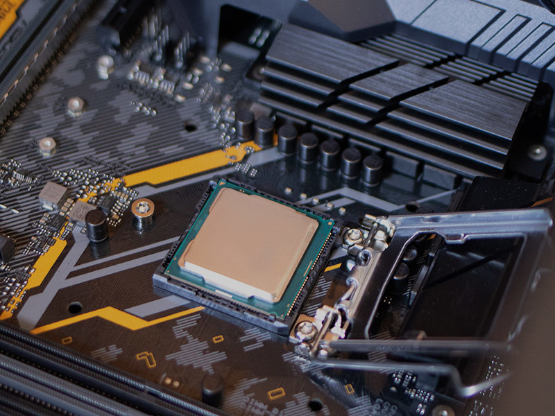
MST provides a complete solution for wafer-level fan-out advanced packaging
Founded in July 2018, MST is a high-tech enterprise dedicated to innovation in wafer-level advanced packaging technologies. We leverage our independently developed and controlled fan-out wafer-level packaging technology platform to deliver high-performance Chiplet integration solutions. With a comprehensive technology portfolio encompassing bumping, WLCSP, fan-out, SiP and 2.5D/3D chiplet integration, we provide global clients with highly reliable and densely integrated advanced packaging services, accelerating the innovation of next-generation high-performance chips.


Fan-Out Wafer-Level Packaging
Three Major Advantages

Performance Advantages
Shorter internal connections significantly improve electrical performance; without the use of a substrate layer, it has significantly superior electrical and thermal performance; flexible design suitable for multi-chip integration and system-in-package, and higher reliability.

Size and Area Advantages
Without the use of existing wire bonding, its internal connections are shorter, and the chip size is reduced; the "disappeared" substrate layer reduces the overall thickness; a wide range of packaging sizes are optional.

Wider Range of Applications
It can realize multi-chip integration, multi-layer wiring interconnection packaging and system-level packaging; flexible design of pin (I/O) quantity; meets the needs of electronic systems for miniaturization, multi-functionality, high performance, high reliability, low cost, and low energy consumption.
Application Areas
We always adhere to the customer first principle, wholeheartedly serving our customers, and insist on using our services to impress customers
SiP Packaging 5G Chips
Explore Details →

Wearable Devices
Explore Details →

Radio Frequency Field (AIoT)
Explore Details →

High-Performance Scenarios (HPC/AI)
Explore Details →
Technical Solutions
MST's Fan-Out north process can achieve a wiring precision of 2-5μm, has the ability to integrate and stack chips with 5-7nm and below nodes, and can meet and provide mass production technology for mobile phone mobile SOC and Chiplet three-dimensional stacked fan-out packaging.
Scalable Hybrid-Pkg
It can flexibly implement BGA/bump methods; It can also be integrated with the substrate as an optimized hybrid package structure.
Sub-um Interconnection
Bridge Si can provide sub-um level interconnection similar to the CoWoS/interposer method; Lower cost compared to CoWoS/Interposer.
Fine pitch FO RDL
Using Face Up FO method; 2um level fine pitch RDL can be achieved, significantly exceeding eWLB solutions.
Unique TMV 3D Interconnection
TMV achieves 2.5D/3D interconnection; Avoids the chip re-design problem required when using TSV solutions.
Contact-less Debonding
Excellent chip mounting and debonding method; Achieve +/-1um level positioning accuracy; Non-destructive optical debonding.
Downward Compatible Common FO
For common FO in conventional application scenarios with >8um linewidth; Adopting a compatible face-down south process to achieve the best cost-effectiveness for customers.
Blog
Here, you can keep abreast of our news and industry information


 Integrated Circuit Co., Ltd.")
Contact Us
Hotline:
Business Contact
Company Address
Office Address:
Building 5, 6th Floor, Haichuang Green Valley Center, No. 1999, YuHang Tang Road, Wuchang Street, Yuhang District, Hangzhou City
Factory Address:
No. 29, Xinchi Road, Chengnan Economic Development Zone, Gaoyou City, Yangzhou City
WeChat Official Account
Follow us
Microsilicon Technology (Gaoyou) Chip Integration Co., Ltd


Copyright © Microsilicon Technology (Gaoyou) Chip Integration Co., Ltd